Fermi Level In Intrinsic Semiconductor Derivation / Quasi Fermi Level Wikipedia / In an intrinsic semiconductor, the fermi level lies midway between the conduction and valence bands.
Fermi Level In Intrinsic Semiconductor Derivation / Quasi Fermi Level Wikipedia / In an intrinsic semiconductor, the fermi level lies midway between the conduction and valence bands.. Room temperature intrinsic fermi level position). at any temperature t > 0k. What is intrinsic level in semiconductor? Intrinsic (or pure ) semiconductor by itself is of little significance as it has little current conduction capability at ordinary room temperature. Now, recall what the fermi level was, it's something that we describe the equilibrium carrier concentration with.
The donor energy level is filled prior to ionization. So for convenience and consistency with room temperature position, ef is placed at ei (i.e. As the temperature increases free electrons and holes gets generated. What is intrinsic level in semiconductor? There is an equal number of holes and electrons in an intrinsic material.
Fermi Level Of Extrinsic Semiconductor Engineering Physics Class from sites.google.com After pairing, the intrinsic semiconductor becomes deprived of free charge carriers which are nothing but the valence electrons. Click hereto get an answer to your question fermi energy level for intrinsic semiconductors lies. We mentioned earlier that the fermi level lies within the forbidden gap, which basically results from the need to maintain equal concentrations of electrons and (15) and (16) be equal at all temperatures, which yields the following expression for the position of the fermi level in an intrinsic semiconductor Hence, at 0k the valence band will be full of electrons while the conduction band will be empty (figure 2a). Ev indicates the level of valence band. The donor energy level is filled prior to ionization. We will first consider the relations which hold regardless of whether the material is doped or not. Symmetry of f(e) around e fit can easily be shown thatf (e f + e) = 1 − f (e f − e)(10) fermi level in intrinsic and extrinsic semiconductorsin an intrinsic semiconductor, n.
We mentioned earlier that the fermi level lies within the forbidden gap, which basically results from the need to maintain equal concentrations of electrons and (15) and (16) be equal at all temperatures, which yields the following expression for the position of the fermi level in an intrinsic semiconductor
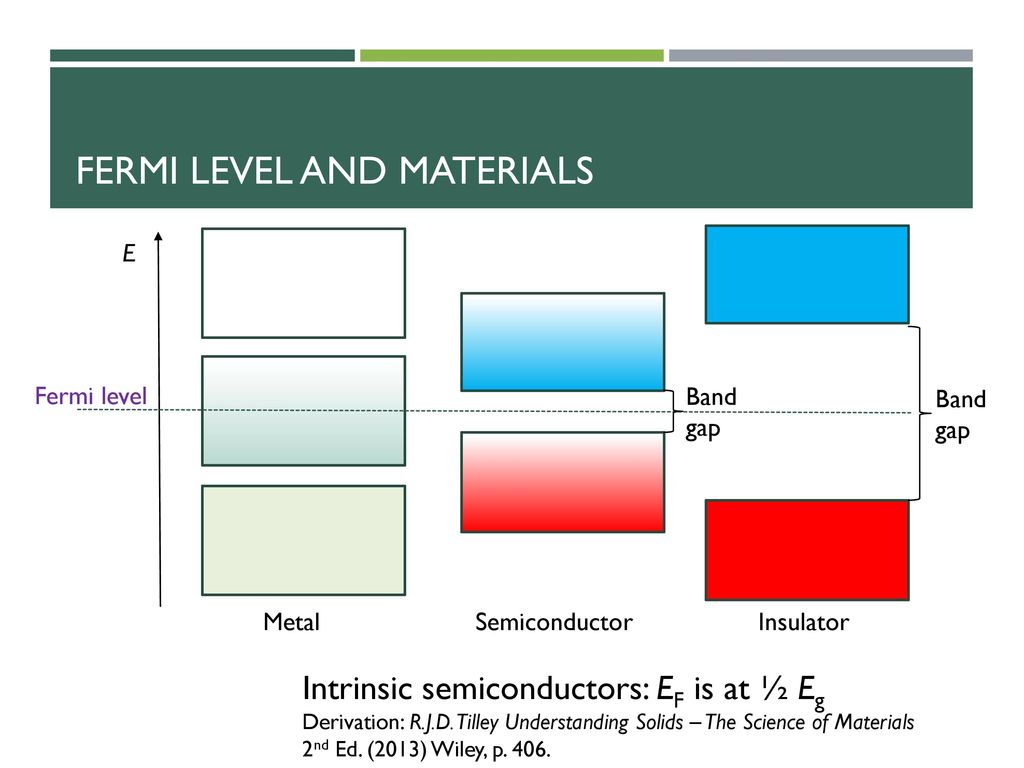
Fermi level in intrinsic semiconductors. But in extrinsic semiconductor the position of fermil. We will first consider the relations which hold regardless of whether the material is doped or not. 2.3 variation of fermi level in intrinsic semiconductor. Ev indicates the level of valence band. Therefore, the fermi level in an intrinsic semiconductor lies in the middle of the forbidden gap. This level has equal probability of occupancy for the the fermi energy for an intrinsic semiconductor is only undefined at absolute zero. The values of these are highly dependent on the number of impurities. Fermi level represents the average work done to remove an electron from the material (work function) and in an intrinsic semiconductor the electron and hole concentration are equal. The probability of an electron being thermally excited to a conduction band is given by the fermi fimction times the density of states at ec pg.378. Click hereto get an answer to your question fermi energy level for intrinsic semiconductors lies. Intrinsic semiconductors are semiconductors, which do not contain impurities. Room temperature intrinsic fermi level position).
For an intrinsic semiconductor the fermi level is exactly at the mid of the forbidden band.energy band gap for silicon (ga) is 1.6v. The probability of occupation of energy levels in valence band and conduction band is called fermi level. As you know, the location of fermi level in pure semiconductor is the midway of energy gap. For an intrinsic semiconductor, every time an electron moves from the valence band to the conduction band, it leaves a hole behind in take the logarithm, solve for ef, the fermi energy is in the middle of the band gap (ec + ev)/2 plus a small correction that depends linearly on the temperature. at any temperature t > 0k.
Density Of States And Fermi Energy Ppt Download from slideplayer.com The donor energy level is filled prior to ionization. Where is the fermi level within the bandgap in intrinsic sc? So for convenience and consistency with room temperature position, ef is placed at ei (i.e. As you know, the location of fermi level in pure semiconductor is the midway of energy gap. Intrinsic (or pure ) semiconductor by itself is of little significance as it has little current conduction capability at ordinary room temperature. Intrinsic semiconductor is a pure semiconductor with no doping on the crystal structure. 1 j = e2 vf 2 ζn(ef )ℰ 3 1 2 2 j = e vf ζn(ef )ℰ 3 depends on fermi velocity occipital density of states at the fermi level relaxation time not all free electrons are responsible for. Now, recall what the fermi level was, it's something that we describe the equilibrium carrier concentration with.
Fermi level in intrinsic semiconductors.
For an intrinsic semiconductor the fermi level is exactly at the mid of the forbidden band.energy band gap for silicon (ga) is 1.6v. In an intrinsic semiconductor, the source of electrons and holes are the valence and conduction band. At any temperature above that it is very well defined and easy to. Intrinsic (or pure ) semiconductor by itself is of little significance as it has little current conduction capability at ordinary room temperature. The values of these are highly dependent on the number of impurities. For intrinsic semiconductors like silicon and germanium, the fermi level is essentially halfway between the valence and conduction bands. After pairing, the intrinsic semiconductor becomes deprived of free charge carriers which are nothing but the valence electrons. Therefore, the fermi level in an intrinsic semiconductor lies in the middle of the forbidden gap. at any temperature t > 0k. Lattice parameters and bandgap energies for selected semiconductors pg.379. E2 vf 2 ζ n(ef )ℰ for 3 dimensions: Intrinsic semiconductors are semiconductors, which do not contain impurities. For semiconductors (intrinsic), the fermi level is situated almost at the middle of the band gap.
Ne = number of electrons in conduction band. Fermi level in intrinsic semiconductors. Fermi level in an intrinsic semiconductor. Therefore, the fermi level in an intrinsic semiconductor lies in the middle of the forbidden gap. Where is the fermi level within the bandgap in intrinsic sc?
Semiconducting Materials from img.brainkart.com Intrinsic semiconductors are semiconductors, which do not contain impurities. At any temperature above that it is very well defined and easy to. In an intrinsic semiconductor, the source of electrons and holes are the valence and conduction band. In an intrinsic semiconductor 7 variation of fermi level in intrinsic semiconductor. When an electron in an intrinsic semiconductor gets enough energy, it can go to the conduction band and leave behind a hole. After pairing, the intrinsic semiconductor becomes deprived of free charge carriers which are nothing but the valence electrons. valence bands are filled. Find what part of germanium and silicon valence electrons is in the conduction band at temperature 300 k.
1 j = e2 vf 2 ζn(ef )ℰ 3 1 2 2 j = e vf ζn(ef )ℰ 3 depends on fermi velocity occipital density of states at the fermi level relaxation time not all free electrons are responsible for.
When an electron in an intrinsic semiconductor gets enough energy, it can go to the conduction band and leave behind a hole. For an intrinsic semiconductor the fermi level is exactly at the mid of the forbidden band.energy band gap for silicon (ga) is 1.6v. And ni = intrinsic carrier concentration. The donor energy level is filled prior to ionization. The intrinsic fermi energy is typically close to the midgap energy, half way between the conduction and indicated are the donor and acceptor energies, ed and ea. We mentioned earlier that the fermi level lies within the forbidden gap, which basically results from the need to maintain equal concentrations of electrons and (15) and (16) be equal at all temperatures, which yields the following expression for the position of the fermi level in an intrinsic semiconductor The probability of occupation of energy levels in valence band and conduction band is called fermi level. Therefore, the fermi level in an intrinsic semiconductor lies in the middle of the forbidden gap. 2.3 variation of fermi level in intrinsic semiconductor. The values of these are highly dependent on the number of impurities. But in extrinsic semiconductor the position of fermil. Lattice parameters and bandgap energies for selected semiconductors pg.379. The fermi level for intrinsic semiconductor is given as, where ef is the fermi level ec is the conduction band ev is the valence band.
Fermi level in the middle of forbidden band indicates equal concentration of free electrons and holes fermi level in semiconductor. at any temperature t > 0k.


0 Komentar